Electronics
PWM Control of 3 LEDs with 1 Wire using Texas Instrument's TLC59731
I/O pins are notorious on short supply on MCU's.
So what do you do if you have only one to spare and a number of chanels you want to PWM control?
I found this little fellow, that only uses one digitial output pin to control a basically infinit number of PWM chanels.
Hardware
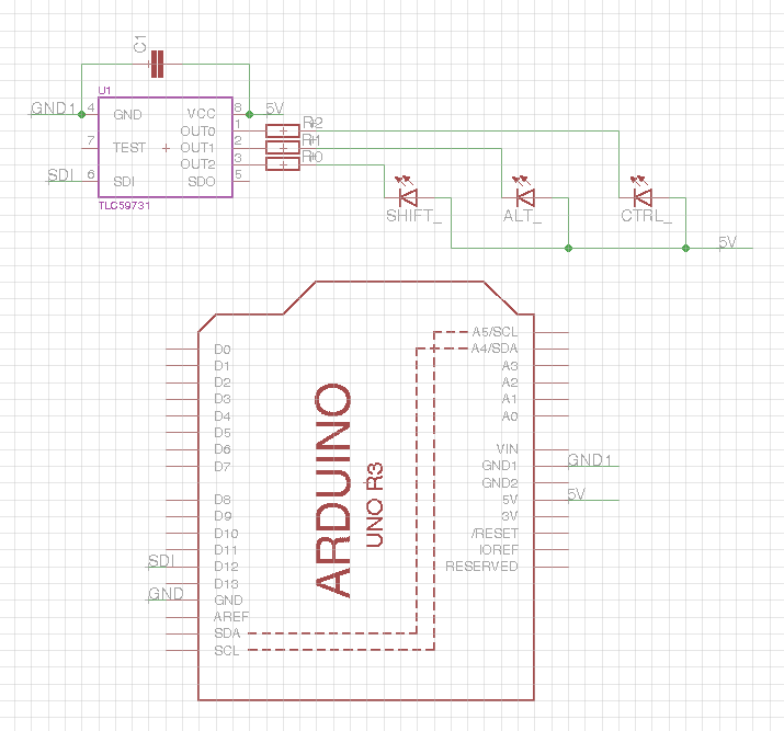
The schematic is simle enough.

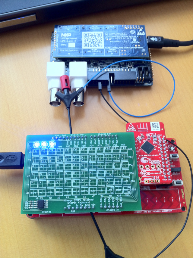
I put the circut on an ARDUINO UNO R3 shield (together with some other suff I'm currently playing around with), shown here sitting on top of a Cypress CY8CKIT-042-BLE Poineer Kit.

Protocol
If you only have one wire to control multiple PWM chanels the complexity has to go into the protocol.
Turns out the protocol is not difficult to understand, only the datasheet of the TLC59731 is (at least was for me).
So I decided to hook up my logic analyser and start playing around with the information of the datasheet.
I find things so much easier to understand if I can see what is going on on the wire.

The wire protocol - It's all about the right timing:
- We start at T with a rising edge.
No bit is transfered at this time. - The time to the next rising edge C1 is measured by the chip.
This is the cycle time for the bit clock (1/fclk). After that time a start pulse for the next bit transfer is expected. - With each consecutive rising edge at 1/fclk a bit transfer is started.
- A logic 0 is transfered, if the line is kept low until the next Bit Transfer Start rising edge at 1/fclk.
(C1 and C2) - A logic 1 is transfered, if the Bit Transfer Start edge is followed by a rising edge before 0.5*(1/fclk).
(C3 and C4)
- A logic 0 is transfered, if the line is kept low until the next Bit Transfer Start rising edge at 1/fclk.
- An End Of Sequence (EOS) is denoted by keeping the line low between 3.5*(1/fclk) and 5.5*(1/fclk).
This is used when multiple chips are daisy chained, to start the data for the next chip.
A new T-C1 sequence is needed to establish a new fclk after each EOS. - Keeping the line low for at least 8*(1/fclk) denotes the Gray Scale Latch (GSLAT) signal. Only now all the chips transfer the bits they received from there 32 Bit Shift Register to there 24 Bit Gray Scale Latch Register, changing the PWM outputs all at the same time (for chips that have received the GS Data Latch Write Command, see below).
The higher protocol:
- Data are transfered Most Significant Bit of Most Significant Byte first down to Least Significant Bit of Least Significant Byte (MSB).
- For each chip 32bit are transferred.
- The eight MSBs are the GS Data Latch Write Command if the value of this byte is 0x3A.
If the value is not 0x3A the PWM outputs of this chip will not change, since no data are written to the GS Latch Register, even if the GSLAT signal is received. - The next 8bit are the GS DATA (PWM) for the GSOUT0 port.
- Followed by the 8bit GS DATA (PWM) for the GSOUT1 port.
- Followed by the 8bit GS DATA (PWM) for the GSOUT2 port.
- After that you send an EOS signal, if you have more than one chip on the line.
- After all bits have been sent to all chips, you send the GSLAT signal, which will switch all GSOUTputs of all chips that received a 0x3A GS Data Latch Write Command, at the same time.
Software
Once understood the protocol is not hard to implement.

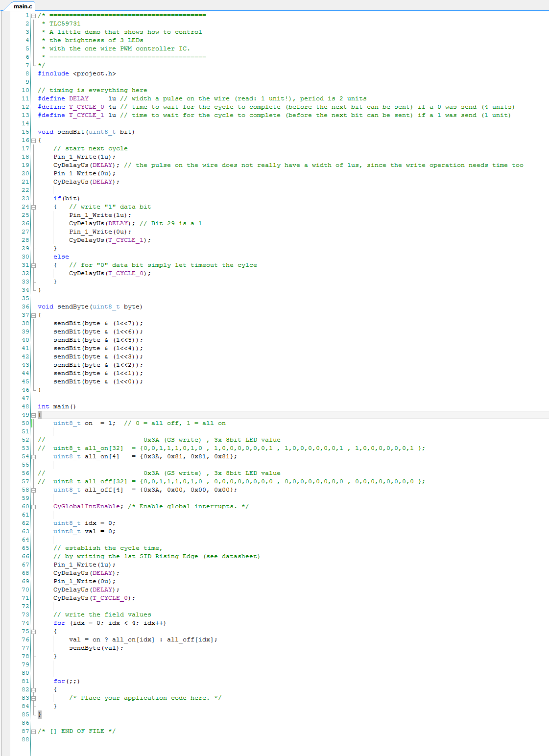
This is the example for the Cypress CY8CKIT-042-BLE, that uses the Cypress CY8C4247LQI-BL483 PSoC.
You can download the source from my GitHub project page. If I have found the time already, you might also find the source for other platforms there.
Source code explained:
- To keep the example straight forward, I did not use any fancy timer interrupt or any serial data transfer for interactive intensity change.
- Lines 10..13 define some constants for delay times. These you might want to adjust to your MCU's speed.
I found that the timing is very roboust, so we don't need to worry about those to much. Especially since the TLC59731 could handle up to 600kHz, while my PSoC only sends at about 95kHz. - Lines 15..34 implement a function that sends one bit over the wire:
- We send the Bit Transfer Start signal, by
- Pulling the line high (line 18)
- Waiting for one time unit (line 19)
- Pulling the line low (line 20)
- Waiting for one time unit (line 21), to complete the pulse.
- If a logic 1 is to be send (
bit!= 0 at line 23), we do so by:- Pulling the line high (line 25)
- Waiting for one time unit (line 26)
- Pulling the line low (line 27)
- Waiting for one time until next 1/fclk is due (line 28).
- If a logic 0 is to be send (
bit== 0 at line 23), we do so by:- Waiting for four time units (until next 1/fclk is due, line 32)
- We send the Bit Transfer Start signal, by
- Lines 36..46 implement a function that sends one byte over the wire:
- We mask out everything except the Most Significant Bit (line 38), by
- By shifting a 1 to the 27 positon of the second operant byte.
- An
ANDoperation withbytesets all other bits inbyteto 0. - The result is !=0 if the 27 bit in byte is 1.
- The result is ==0 if the 27 bit in byte is 0.
- This result is send using the
sendBit()function (line 38). - We use the same concept to send all bits of
bytein the correct order (lines 39..45).
- We mask out everything except the Most Significant Bit (line 38), by
- Lines 48..85 implement the
main()function:- The variable
onis defined.- Setting
onto 1 will switch all LEDs on. - Setting
onto 0 will switch all LEDs off.
- Setting
- The field
onis defined, that holds the bytes to be send to switch all LEDs on.- At index 0 you find the GS Data Latch Write command byte 0x3A.
- The remaining positions (index 1..3) hold the three LED PWM value bytes (0x81 for a 47% duty cycle, s. page 13 of the datasheet).
You have to change these values to change the brightness of the LEDs.
- The field
offis defined, that holds the bytes to be send to switch all LEDs off. - Ignore line 60, it is boiler plate code.
- Line 62 defines an index variable, we use later to iterate through the
onorofffield. - Line 63 defines a variable to temporarily store the value we found at field
[idx].
- The variable
- Lines 74..78 finally transfer the data:
- We send the "ping" at T (lines 68..71), upfront the data transfer to establish fclk.
- The lines 74..78 loop through
idx0..3:- If
on!= 0,valis assigned the value fromon[idx]. - If
on== 0,valis assigned the value fromoff[idx]. valis send over the wire by calling the functionsendByte().
- If
- Since nothing more happens on the wire after that, we time out 8*(1/fclk), which is the GSLAT signal for the TLC59731, that updates the PWM outputs.
The pictures above show the results of this program.